- 您现在的位置:买卖IC网 > Sheet目录342 > MC34845AEPR2 (Freescale Semiconductor)IC LED DVR BACKLIGHT 6CH 24QFN
ELECTRICAL CHARACTERISTICS
ABSOLUTE MAXIMUM RATINGS
ELECTRICAL CHARACTERISTICS
ABSOLUTE MAXIMUM RATINGS
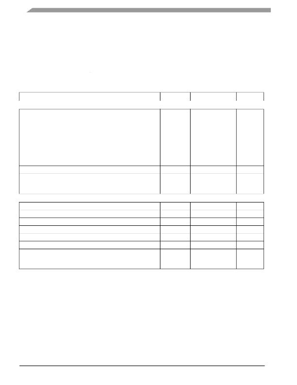
Table 2. Absolute Maximum Ratings
All voltages are with respect to ground unless otherwise noted. Exceeding these ratings may cause a malfunction or
permanent damage to the device.
Ratings
Symbol
Value
Unit
ELECTRICAL RATINGS
Maximum Pin Voltages
SWA, SWB, VOUT
CH1, CH2, CH3, CH4, CH5, CH6 (Off state)
CH1, CH2, CH3, CH4, CH5, CH6 (On state)
FAIL
OVP
COMP, ISET
PWM, WAKE
EN, VIN
V MAX
-0.3 to 65
-0.3 to 45
-0.3 to 20
-0.3 to 7.0
-0.3 to 7.75
-0.3 to 2.7
-0.3 to 5.5
-0.3 to 24
V
Maximum LED Current per Channel
I LED_MAX
33
mA
ESD Voltage
(1)
V ESD
V
Human Body Model (HBM)
Machine Model (MM)
THERMAL RATINGS
± 2000
± 200
Operating Ambient Temperature Range
Maximum Junction Temperature
Storage Temperature Range
T A
T J
T S
-40 to 85
150
-40 to 150
°C
°C
°C
Peak Package Reflow Temperature During Reflow
(2) , (3)
T PPRT
Note 3
°C
Thermal Resistance Junction to
Thermal Resistance Junction to
(4)
Power Dissipation
Ambient (4)
Case (5)
T θ JA
T θ JC
P D
36
3.1
°C/W
°C/W
W
TA = 25°C
TA = 85°C
3.4
1.8
Notes
1. ESD testing is performed in accordance with the Human Body Model (HBM) (AEC-Q100-2) (C ZAP = 100 pF, R ZAP = 1500 Ω ), and the
Machine Model (MM) (C ZAP = 200 pF, R ZAP = 0 Ω.
2.
3.
4.
5.
Pin soldering temperature limit is for 10 seconds maximum duration. Not designed for immersion soldering. Exceeding these limits may
cause malfunction or permanent damage to the device.
Freescale’s Package Reflow capability meets Pb-free requirements for JEDEC standard J-STD-020C. For Peak Package Reflow
Temperature and Moisture Sensitivity Levels (MSL), Go to www.freescale.com, search by part number [e.g. remove prefixes/suffixes
and enter the core ID to view all orderable parts. (i.e. MC33xxxD enter 33xxx), and review parametrics.
Per JEDEC51-8 Standard for Multilayer PCB
Theoretical thermal resistance is from the die junction to the exposed pad.
34845
Analog Integrated Circuit Device Data
4
Freescale Semiconductor
发布紧急采购,3分钟左右您将得到回复。
相关PDF资料
MC34845BEPR2
IC LED DVR BACKLIGHT 6CH 24QFN
MC34848EPR2
IC LED DVR BACKLIGHT 8CH 48QFN
MC56F8006DEMO-T
BOARD DEMO FOR MC56F8006 DSP
MCB1114
BOARD EVALUATION FOR NXP LPC1114
MCB11C14
BOARD EVAL FOR NXP LPC11C14
MCB2470
BOARD EVAL NXP LPC247X SERIES
MCBSTM32EXL
BOARD EVALUATION FOR STM32F103ZE
MCBTMPM330
BOARD EVAL TOSHIBA TMPM330 SER
相关代理商/技术参数
MC34845BEP
功能描述:USB 接口集成电路 6-Ch LED Backlt Driver RoHS:否 制造商:Cypress Semiconductor 产品:USB 2.0 数据速率: 接口类型:SPI 工作电源电压:3.15 V to 3.45 V 工作电源电流: 最大工作温度:+ 85 C 安装风格:SMD/SMT 封装 / 箱体:WLCSP-20
MC34845BEPR2
功能描述:USB 接口集成电路 6-Ch LED Backlt Driver RoHS:否 制造商:Cypress Semiconductor 产品:USB 2.0 数据速率: 接口类型:SPI 工作电源电压:3.15 V to 3.45 V 工作电源电流: 最大工作温度:+ 85 C 安装风格:SMD/SMT 封装 / 箱体:WLCSP-20
MC34845CEP
功能描述:LED照明驱动器 6-Ch LED Backlt Driver RoHS:否 制造商:STMicroelectronics 输入电压:11.5 V to 23 V 工作频率: 最大电源电流:1.7 mA 输出电流: 最大工作温度: 安装风格:SMD/SMT 封装 / 箱体:SO-16N
MC34845CEPR2
功能描述:LED照明驱动器 6-Ch LED Backlt Driver RoHS:否 制造商:STMicroelectronics 输入电压:11.5 V to 23 V 工作频率: 最大电源电流:1.7 mA 输出电流: 最大工作温度: 安装风格:SMD/SMT 封装 / 箱体:SO-16N
MC34845DEP
功能描述:LED照明驱动器 6-Ch LED Backlt Driver RoHS:否 制造商:STMicroelectronics 输入电压:11.5 V to 23 V 工作频率: 最大电源电流:1.7 mA 输出电流: 最大工作温度: 安装风格:SMD/SMT 封装 / 箱体:SO-16N
MC34845DEPR2
功能描述:LED照明驱动器 6-Ch LED Backlt Driver RoHS:否 制造商:STMicroelectronics 输入电压:11.5 V to 23 V 工作频率: 最大电源电流:1.7 mA 输出电流: 最大工作温度: 安装风格:SMD/SMT 封装 / 箱体:SO-16N
MC34845EP
功能描述:LED照明驱动器 6-Ch LED Backlt Driver RoHS:否 制造商:STMicroelectronics 输入电压:11.5 V to 23 V 工作频率: 最大电源电流:1.7 mA 输出电流: 最大工作温度: 安装风格:SMD/SMT 封装 / 箱体:SO-16N
MC34845EPR2
功能描述:LED照明驱动器 6-Ch LED Backlt Driver RoHS:否 制造商:STMicroelectronics 输入电压:11.5 V to 23 V 工作频率: 最大电源电流:1.7 mA 输出电流: 最大工作温度: 安装风格:SMD/SMT 封装 / 箱体:SO-16N
